
Wafer Back Grinding Process تولید کننده درک توانایی تولید قوی ، قدرت تحقیق پیشرفته و خدمات عالی ، شانگهای Wafer Back Grinding Process تأمین کننده ارزش ایجاد می کند و برای همه مشتری ارزش ایجاد می کند.
Standard Back Grind Norton ... cost has forced wafer fabs to optimize the back grinding process to improve yield. An important factor is the wafer strength after back ...
Plasma systems for wafer stress relief ... process containing no free ions or electrons that could potentially charge the surface of the wafer. The backgrinding ...
Because the thinning of the whole wafer at the back ... use a twostep process including a coarse grinding ... Wafer Thinning: Techniques for Ultrathin Wafers ...
Effect of Wafer Back Grinding on the Mechanical Behavior of Multilayered Lowk for 3DStack Packaging ... generated during wafer back grinding process affect the
This is an advanced back grinding tape laminator for thin wafers that achieves tensionfree lamination. The lineup consists of two product types that vary in ...
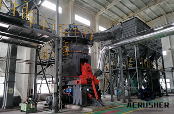
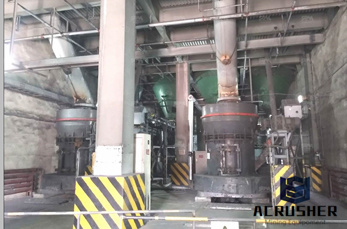
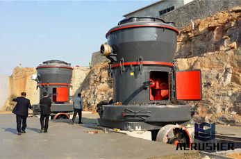
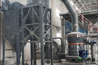
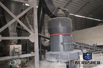
Home / Products / Grinding Process Wafers. ... Back Grinding For Bare Device Patterned Wafers,SVM,Inc. Back grinding is a process that removes silicon from the back ...
GDSI, Grinding and Dicing Services complete resource for Silicon Wafers Processing includes Probing, Bumping, Grinding, Polishing in San Jose, California.
One is slicing the silicon ingot, the other is wafer back grinding after circuit process is completed. ... How thin can we cut silicon wafers? Update Cancel.
BackSide Wafer Grinding Quality Affecting BackEnd Assembly, back grinding process,ABSTRACT Die size and thickness of IC substrate typically vary as a .
The TAIKO process is the name of a wafer back grinding process that uses a new grinding method developed by DISCO This method is different to conventional back ...
World leading Technology for grinding/thinning of wafer ... fine grinding of prime wafers or back ... grinding process efficiency. Prime wafer ...
Syagrus Systems thin wafer backgrinding and silicon wafer thinning services meets ... more about our Wafer Dicing Process. ... your next back grinding wafer ...
ICROS TAPE is used to manufacture integrated circuits as a surface protective tape in the silicon wafer backgrinding process.
The TAIKO process is the name of a wafer back grinding process that uses a new grinding method developed by DISCO. This method is different to conventional back grinding.
Leadingedge Tape B!_ (B Equipment solution created with semiconductorrelated products ''Adwill.'' Fully and semiautomatic wafer mounters for the dicing process.
A wafer sawing/grinding process capable of removing cracks and chipping resulted from a wafer sawing operation. A silicon wafer having an active surface and a back ...
Semiconductor BackGrinding The silicon wafer on which the active elements are created is a thin circular disc, typically 150mm or 200mm in diameter.
Warping of silicon wafers subjected to backgrinding process. This study investigates warping of silicon wafers in ultraprecision grindingbased backthinning process.
Wafer Backgrind is the process of grinding the backside of the wafer to the correct wafer thickness prior to assembly. It is also referred to as ''wafer ...
Semiconductor Wafer Edge Analysis/4 Stricter requirements in the wafer manufacturing process have made edge measurements important for both 200 mm and 300 mm wafers.
wafer back grinding process Products for Back Grinding Process This is an advanced back grinding tape laminator for thin wafers that achieves tensionfree lamination ...
Introduction of Product Introduction of Wafer Surface Grinding Machine Model GCG300 Junichi Y amazaki Meeting the market requirements for silicon wafers .
Wafer Service Overview; ... glass support substrates and wafers. Grinding stresses on the wafer are ... 3/features/thebackendprocessstep3wafer ...
Wafer backgrinding or Wafer Thinning; ... During the wafer thinning process, wafers are commonly thinned to thicknesses of 75 to 50 microns.
 WhatsApp)